
This website explains how the algorithm worked in the IBM system/360 Model 91 and how the HASE model works.
The files for this model can be downloaded as a zip file from tomasulo_v1.8.zip
Instructions on how to use HASE models can be found at Downloading, Installing and Using HASE.
One of the problems facing the designers of high-speed computer systems at the time was the difficulty of achieving the fastest possible execution times for a particular technology in universal execution units. Circuitry designed to carry out both multiplication and addition, for example, could do neither as fast as two units each limited to one kind of operation. Thus not only did the Model 91 contain separate fixed-point and floating-point execution areas, but the floating-point area contained separate add and multiply/divide units capable of concurrent operation. Although both units were internally pipelined, only the add unit (a two-stage pipeline) could start a new operation in each (60 ns) clock cycle. The multiply/divide unit took three cycles to execute a multiply and 12 cycles to execute a divide, but could only deal with one instruction at a time.
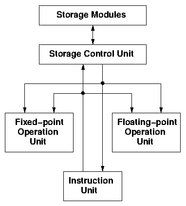
Figure 1. The IBM System/360 Model 91 Processsor
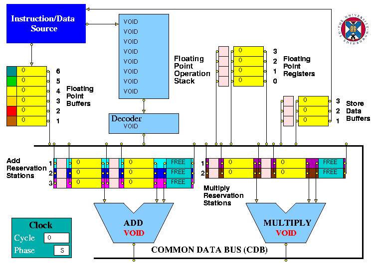
Figure 2. The HASE Tomasulo's Algorithm model
Instructions in the Source memory can be of the form:
| LOAD | Fx | memory address |
| STORE | Fx | memory address |
| ADDRR | Fx | Fy |
| ADDRS | Fx | memory address |
| SUBRR | Fx | Fy |
| SUBRS | Fx | memory address |
| MULRR | Fx | Fy |
| MULRS | Fx | memory address |
| DIVRR | Fx | Fy |
| DIVRS | Fx | memory address |
| STOP 0 |
where Fx and Fy are floating-point registers, RR implies a register-register operation and RS a register-storage operation. The IBM System/360 used a two-address instruction format, so that ADDRR Fx Fy, for example, executes:
| Fx | = | Fx | + | Fy |
The corresponding pseudo instructions are of the form:
| LD | Fx | FLBy |
| ST | Fx | SDBy |
| ADD | Fx | Fy |
| ADD | Fx | FLBy |
| etc |
where SDB is a Store Data Buffer. Whenever the Source decodes a STORE instruction it enters the memory address into a local table and, when it receives an input from an SDB, looks up the corresponding address and writes the result into the data memory. Like the FLBs, SDBs are allocated cyclicly, but unlike the FLBs, a separate busy bit is maintained in the Source unit for each SDB since results may come back out of order. If all three are busy, the Source waits until one is free before issuing another STORE order. When a STOP instruction is encountered (in the model the instruction sequence must always end in a STOP), the Source waits until all three SDBs are free before issuing the STOP to the FLOS.
The instructions and data used by the model are in the files SOURCE.instr_mem.mem and SOURCE.data_mem.mem. The user's copies of these files can be edited to try out different programs. The Source Unit checks that instruction and data addresses fall within the range of addresses defined by the memory sizes in the .edl file; if an out-of-range address is found the simulation is stopped and an error message is displayed in the Output pane.
In ClockPhase0 entities other than the Common Data Bus execute whatever operations are appropriate in response to their inputs and in ClockPhase1 send the results of their operations to the next entity. Since the principal actions of the Common Data Bus are to pass tags and data between other entities, it does this in ClockPhase0.
Each ClockPhase lasts for 10 simulation time steps. This allows actions occurring within a ClockPhase to be sequenced. Within the Decoder, ClockPhase0 is effectively split into two subphases, each lasting for 5 simulation time steps. This allows tag updates resulting from tag and data movements on the Common Data Bus to be completed before the Decoder uses the information in its tag table to determine its actions for the instruction it is currently decoding.
In ClockPhase1, provided that the Decoder has acknowleded the previous instruction sent to it, the instruction in element 0 is read out and, unless it is a VOID, sent to the Decoder. The remaining instructions in the queue are then moved down one position and if the the pointer has a value greater than 0, its value is decremented.
An LD instruction takes an operand from an FLB (Floating-point Buffer) and sends it to an FLR (Floating-point Register). The Decoder determines the FLB number and invokes a class in this FLB telling it to send its operand to the CDB. The FLB sets an internal flag so that if it has already received an operand (and tag number) in a packet from the Source, it will send the operand value and tag number in a packet to the CDB in the subsequent ClockPhase1. If it has not received a packet from the Source, it will wait until it has and then send its operand and tag number in the next ClockPhase1. In either case, after sending the packet to the CDB, the FLB resets its flag and sets its operand value to zero.
The Decoder also sends a tag packet (not shown in the animation) to the relevant FLR tag register. The FLR tag register changes state to display the colour corresponding to the tag it has received.
An ST instruction takes an operand from an FLR and sends it to an SDB (Store Data Buffer). The Decoder determines the FLR number and checks its tag value. If the tag is zero, it invokes a class in this FLR telling it to send its operand to the CDB in ClockPhase1. If the tag is non-zero it copies this tag to the relevant SDB tag table entry. The CDB sends a packet to the relevant SDB tag register.
The roles of Sink and Source are reversed for an ST instruction, i.e. the Source is an FLR, determined by the sink field in the instruction and the Sink is the SDB, determined by source field.
For a STOP instruction, the Source unit takes special action. It checks for outstanding ST instructions and only sends the STOP instruction to the FLOS when it hase received all outstanding SDB results. The Decoder tests for non-zero tags when it receievs a STOP instruction. If any tag is non-zero, it waits until the next clock cycle and repeats the check. Once all tags have become zero, the Decoder sends a stop signal to the clock to end the simulation.
For arithmetic functions the Decoder first decides which arithmetic unit is required and then selects a free Reservation Station. The Decoder contains the Busy Bits for these Stations and sets the Busy Bit of the selected Station. The Busy Bit is reset by the Reservation Station when its operands have been sent to the relevant Arithmetic Unit.
Once it has allocated a Reservation Station, the Decoder checks the state of the Tags for the Sink and Source operands (the Tag table is contained within the Decoder, the tag registers on the screen being used solely for display purposes). In the IBM System/360 Model 91, a separate busy bit was associated with each FLR. In the HASE model, the busy state is determined by whether the associated tag register contains a zero or non-zero value. Thus if the Tag is zero, a class is invoked in the relevant FLR entity telling it to send its operand to the CDB (in the next ClockPhase1) and which Reservation Station register it is destined for.
Requests from the Decoder, Add and Multiply units can only be dealt with one at a time. In the original IBM scheme, the Add unit, for example, had to give notice that it was going to produce a result two clock cycles ahead of time. In the HASE model each sending unit enters a Held state and only frees when it gets an acknowledge from the CDB. The CDB deals with simultaneous requests in successive clock periods in the following priority order: Multiply, Add, Decoder.
Request packets from the Decoder contain the following fields:
The CDB uses the Sink Reservation Station register number to select the RS Control register to which it will send the instruction along with the RS Tag number which will be copied through the arithmetic unit and presented to the CDB with the result operand.
If the Sink/Source Tag number is zero, the CDB extracts the Sink/Source operand from the packet sent by the FLR and later sends it to the appropriate RS register. If the Tag is non-zero, it will send the corresponding Tag to the Tag display register (the Decoder will have updated the Tag Array). Before sending either an operand or a Tag, however, the CDB checks the contents of any FLB, Add or Multipier packets it may have received in the same clock.
When an input packet is received from a Floating-point Buffer, the CDB first checks the tags in any current FLR packets. If the FLB tag matches a Sink/Source tag in a waiting packet, the CDB copies the FLB operand into the Sink/Source operand field in the waiting packet, sets the corresponding tag field to zero and updates the Decoder Tag Array for that Sink/Source.
The CDB then checks the FLB tag value against each of the entries in the Tag Array in the Decoder and, if the there is a match, sends the FLB operand to the corresponding register. At the same time it resets that Tag Array entry to zero and sends a packet to the corresponding Tag Display Register (which resets the displayed Tag to the zero state).
When an input packet is received from an arithmetic unit, the CDB first selects the one with higher priority (if there are two), then checks the tags in any packets waiting to go the Reservation Stations or Store Data Buffers (and updates them if necessary) and then checks the arithmetic unit tag against the tags in the Decoder Tag Array. If there is a match it prepares to send the operand and tag to the corresponding operand and tag display registers and resets the entry in the Tag Array to zero.
Once all the checks any packet updates have been completed, the CDB sends any waiting instructions, operands and/or tags to their destinations. Whenever an instruction or operand is sent to a Reservation Station register, the CDB notifies the relevant Reservation Station entity, which monitors the state of the RS registers. If the instruction and operand registers are all full for a particular RS, its contents can be sent to the corresponding arithmetic unit.
When the Common Data Bus sends an instrucion to a Reservation Station, the Control Register receives a packet from the CDB containing an instruction and a tag number, the latter being the number of the Reservation Station. The Control Register displays the function field of the instruction. If the operands are available, they are sent to the Operand registers, which change state and display their operand values. If an operand is not available, the tag for that operand is sent to the corresponding tag register. When a result is subsequently sent to the Common Data Bus containing that tag, the waiting Operand Register receives its operand and changes state accordingly. At the same time, its tag register is returned to the zero state.
As each Reservation Station register receives a packet from the Common Data Bus, the appropriate Add or Multiply/Divide Reservation Station entity itself is notified that the register is ready. The Reservation Station entities monitor the states of their individual Control and Operand registers and when all three registers in one Reservation Station become full, the Reservation Station entity invokes a method in these registers telling them to send their contents to their outputs (from whence they go to the appropriate Arithmetic Unit). If more than one Add or one Multiply Reservation Station becomes full in any one clock period, the operation in the Station with the lowest station number is processed first. The Control Register sends both its function and tag value. The tag is copied through to the output of the arithmetic unit where it appears as the result tag.
The Control Register continues to display its function until the result of that function has been sent to its destination and the corresponding reservation station Busy Bit has been reset in the Decoder, after which it returns to the FREE state. The Operand Registers return to the idle state as soon as they have sent their operands to their arithmetic unit and reset their operand values to zero.
| (1 < add_latency =< 8) |
The Unit is implemented as an 8-stage pipeline, and can accept another instruction in each clock period. It computes its result in the first stage and simply copies it through the remaining stages. The result is taken from the stage corresponding to the latency and sent to the CDB, i.e. if the latency is <8, the remaining pipeline stages are ignored.
| (1 < mul_latency =< 8) |
| (1 < div_latency =< 16). |
The Unit is implemented as a 16-stage pipeline, although it cannot accept another instruction until it has sent the result of an existing instruction to the CDB. It computes its result in the first stage and simply copies this result through the remaining stages. The result is taken from the stage corresponding to function's latency and sent to the CDB.
At the start of a DIV, the unit checks for divide by zero and, if a zero is found, the simulation is stopped and an error message is displayed in the Output pane.
| Program instructions | Pseudo instructions |
|---|---|
| LOAD F0 0 | LD F0 FLB1 |
| LOAD F1 2 | LD F1 FLB2 |
| MULRS F1 3 | MUL F1 FLB3 |
| ADDRR F0 F1 | ADD F0 F1 |
| LOAD F2 4 | LD F2 FLB4 |
| MULRS F2 5 | MUL F2 FLB5 |
| ADDRR F0 F2 | ADD F0 F2 |
| LOAD F3 6 | LD F3 FLB6 |
| MULRS F3 7 | MUL F3 FLB1 |
| ADDRR F0 F3 | ADD F0 F3 |
| LOAD F1 8 | LD F1 FLB2 |
| MULRS F1 9 | MUL F1 FLB3 |
| ADDRR F0 F1 | ADD F0 F1 |
| STORE F0 1 | ST F0 SDB1 |
| STOP 0 | STOP 0 |
As the program executes, the following actions occur in the system:
Return to Computer Architecture Simulation Models