Computer Architecture Simulation & Visualisation
Return to Computer Architecture Simulation Models

EMMA
Edinburgh Microcoded Microprocessor Architecture
EMMA is a HASE simulation model of a simple load/store,
register-register arithmetic microprocessor architecture designed for
use in virtual laboratory exercises in computer design. The processor
has a predefined instruction set but the down-loadable version of the
model contains almost none of the microcode required to implement it.
Instructors can propose exercises in which students write microcode to
implement all or parts of the instruction set together with assembly
code programs to demonstrate that the microcode operates correctly.
When EMMA was originally created in 2005, there were two versions, a
basic version (EMMA-1), that could execute simple arithmetic and logic
operations, and an enhanced version (EMMA-2), that contained
facilities to allow multiplication and division to be implemented in
microcode. The current version (EMMA-3) is a revised version of
EMMA-2, capable of executing the full EMMA instruction set. The
revisions include a change in the way the microinstructions are
represented, from an 8-digit hexadecimal value to a string of 8
hexadecimal characters, so as to provide better visualisation.
This website describes the architecture of EMMA, its instruction
set and microcode, and how to use the model. The files for EMMA-3 can
be downloaded
from EMMA-3.zip.
Instructions on how to use HASE models can be found at
Downloading, Installing and Using HASE.
The original EMMA website and models can be
found here.
EMMA-3 Processor Architecture
EMMA-3 is a simple load/store, register-register arithmetic processor
implemented as shown in Figures 1. It uses a Harvard architecture,
with separate instruction and data memories. The Program Counter (PC)
acts as the memory address register for the Instruction Memory.
Whenever PC receives an update command from the Microprogram Unit, it
sends the new address to the Instruction Memory. The instruction read
out from the Instruction Memory is sent to the Microcode unit where it
is copied into the Instruction Register (IR).
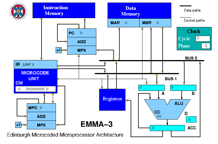
Figure 1. The EMMA-3 simulation model
The Microcode Unit contains the Microcode Memory which is addressed by
the function field of the Instruction Register in the clock cycle in
which a new instruction is received from the Instruction Memory and by
the Microcode Program Counter (MPC) in subsequent clock cycles. If the
Microcode Unit receives an input from both the Instruction Memory and
the Microcode Program Counter in the same clock cycle, the input from
the Microcode Program Counter is discarded (this can happen during the
execution of branch instructions) and a statement to this effect
appears in the Output Pane of the HASE window.
Words in the Microcode Memory are strucured as follows:
| Label | Microinstruction | Operand |
The Label is a string of characters used only for readability
purposes.
The Microinstruction is a string of 8 characters representing a set of
hexadecimal digits that can be interpreted in one of two different
ways according to which half of the 256-word Microcode Memory it is
stored in. Microcode words stored in the least significant half of the
Microcode Memory are interpreted as being in M-Format, in which two of
the hex digits control the Microcode Unit itself, one controls the MPC
Unit, one the PC Unit, one the Registers, one the Data Memory and two
the ALU. Microcode words stored in the most significant half of the
Microcode Memory are interpreted as being in A-Format, in which the
hex digit used to control the Data Memory in M-Format is instead used
to provide extra control signals for the ALU (see Table 3 below).
The (8-bit integer) Operand field is used for jumps within the
microcode memory or as an operand value for some
microinstructions. The first 32 locations form a jump table indexed by
the Function Number (see Table 2 below), except for locations 0 and 1
which each contain the (one) microcode word needed to implement the
JUMP and BRANCH instruction.
EMMA operates on a two phase clock. In clock cycles in which they are
active, each unit executes its internal actions in the first phase of
the clock and sends out a result packet in the second phase. The
Microcode Unit, for example, reads its microcode memory in the first
phase and in the second phase sends the appropriate microcode fields
to other units, if they are to be activated in the next clock
cycle.
The Program Counter and Microprogram Counter units behave identically.
They contain the relevant register together with an adder which
receives one of its inputs from the register itself and the other from
a multiplexer (MPX) which selects either +1 or a value taken from BUS2
in the case of PC or from the Microcode Unit in the case of MPC. (The
+1 value is actually an internal connection, the +1 units are just
included for visual clarity.) Each has two outputs: Output1, which is
connected back to the adder and is permanently enabled, and Output2
which is enabled under microcode control. The bits in the microcode
field controlling the Program Counter, for example, activate its
inputs and output as follows:
| Signal | Connection |
| Input1 | From PC |
| Input2 | +1 |
| Input3 | From BUS2 |
| Output2 | To Instruction Memory |
Whenever the PC unit is activated by receipt of a microcode packet in
one clock cycle (it should also have received appropriate data
packets), it activates the appropriate inputs to the multiplexer and
the adder and forms the result in phase 0 of the next clock cycle; in
phase 1 of that clock cycle it sends the result of the addition to
Output1, back to its own Input1, (always) and to Output2 if the
corresponding microcode bit is set.
The buses (BUS1 and BUS2) have a number of input connections but
should receive data from only one of them in any one (phase 1) clock
period. Inputs which do not receive data are set to zero. The inputs
are internally ORed together (simulating a wired-OR bus) and the
result is sent to all the outputs half way through the clock phase in
which they were received.
The Data Memory has its own built-in Memory Address Register (MAR) and
Memory Buffer Register (MBR). The microcode field controlling the
memory is as follows:
| Signal | Connection |
| MAR Input | From BUS2 |
| MBR Input | From BUS1 |
| Read/Write | |
| MBR Output | To BUS1 |
For a read operation (Read/Write = 0), the address sent from BUS2 is
copied into MAR in the next clock phase 0, the memory is read and the
result copied into MBR. In the subsequent clock phase 1, the value in
MBR is sent to BUS1. For a write operation (Read/Write = 1), the
address sent from BUS2 is copied into MAR in the next clock phase 0,
the data value sent from BUS1 is copied into MBR and the value is
written into the memory.
The Registers unit contains 16 general purpose registers, with R0
being permanently set to 0. It receives input values from the ALU and
has two outputs connected to BUS1 and BUS2. Whenever the Microcode
Unit sends a microcode command to the Registers unit, it appends the
appropriate source and destination register numbers extracted from the
instruction in IR. The microcode field controlling the registers is
as follows:
| Signal | Connection |
| Swap | |
| Input1 (to RD) | From ALU |
| Output1 (RS1) | To BUS1 |
| Output2 (RS2) | To BUS2 |
Executing an instruction such as ADD RD RS1 RS2 requires the execution
of 3 microinstructions. The first microinstruction reads the values in
registers RS1 and RS2 and sends them to BUS1 and BUS2
respectively. This is achieved by setting the Registers field in the
microcode word to 0011. The second microinstruction controls the
adder, while the third causes the result sent from the adder to the
Registers to be written into RD. This microinstruction also
increments the Program Counter. If the Swap bit is set, however, then
the first microinstruction sends the value in RD to BUS2 instead of
RS2 and the third microinstruction writes the result from the adder
into RS1. This facility allows for the implementation in microcode of
complex instructions such as forming the sum of the first n
natural numbers.
The Arithmetic and Logic Unit (ALU) has two data inputs, one each from
BUS1 and BUS2. Values received from the buses are loaded into
registers A and B. The result of an operation is loaded into the
Accumulator (ACC), which has two external outputs, one connected to the
Registers Unit and one to BUS2, and one internal connection back into
the ALU. When the Microcode Unit sends a microcode command to the
ALU, it appends the appropriate function code derived from the
instruction in IR. There are two condition code bits: CC0 is set = 0
if the ALU result = 0; CC1 is set = 1 if the ALU result < 0. CC0 and
CC1 are directly connected to the Microcode Unit which can use them in
condition tests in the clock period after an ALU operation has been
executed.
Eight Basic Functions are provided in the ALU, as shown in Table 1
below, together with eight Extra Functions that allow for the
implementation of multiplication and division in microcode. Four of
these extra functions operate on the A and B registers. The D register
is intended for use in counting down the number of cycles during
division.
| Fn | Action |
| 0 | Add |
| 1 | Subtract |
| 2 | AND |
| 3 | OR |
| 4 | XOR |
| 5 | Shift Left Logical |
| 6 | Shift Right Logical |
| 7 | Shift Right Arithmetic |
Basic Functions
| |
| Fn | Action |
| 8 | NOP (No Operation) |
| 9 | Reverse Subtract |
| A | Negate A |
| B | Negate B |
| C | Shift A Right & set CC |
| D | Shift B Left |
| E | Set D = Operand |
| F | Decrement D & set CC |
Extra Functions
|
Table 1. ALU Functions
The EMMA Instruction Set
Table 2 shows the instructions which the EMMA microcode is expected
to implement. The instruction set includes absolute jumps (JUMP and
JREG) and relative branches (BRANCH, BEQZ and BNEG), loads (LD, LDL, LDX)
and stores (ST and STX), register-register operations (ADD, etc) and
register-literal arithmetic operations (ADDL, etc). There are also two
undefined arithmetic operations (OP1 and OP2) and a STOP instruction
that stops the simulation. All Literal (Immediate) operands are
treated as 16-bit signed integers, i.e. any literal values
which require >16 bits for their representation are truncated and sign
extended to the 32-bit representation used by the adders.
When downloaded, the model files include a MICROCODE.Microcode.mem file
that contains microcode for the JUMP and LD instructions. The first
32 locations of the microcode memory are used as a jump table, indexed
by the function number (except for location 0, which contains the
single microcode word required to implement the JUMP instruction).
Function
Number | Instruction | Action |
| 00 | JUMP Literal | PC = Literal |
| 01 | BRANCH Literal | PC = PC + Literal |
| 02 | BEQZ Literal | If CC0 = 0, PC = PC + Literal
else PC = PC + 1 |
| 03 | BNEG Literal | If CC1 = 1, PC = PC + Literal
else PC = PC + 1 |
| 04 | JREG RS | PC = RS |
| 05 | LD RD Address | RD = Memory[Address] |
| 06 | LDL RD Literal | RD = Literal |
| 07 | LDX RD Address(RS) | RD = Memory[Address+RS] |
| 08 | ST Address RS | Memory[Address] = RS |
| 09 | STX Address(RS2) RS1 | Memory[Address+RS2] = RS1 |
| 10 | ADD RD RS1 RS2 | RD = RS1 + RS2 |
| 11 | ADDL RD RS1 Literal | RD = RS1 + Literal |
| 12 | SUB RD RS1 RS2 | RD = RS1 - RS2 |
| 13 | SUBL RD RS1 Literal | RD = RS1 - Literal |
| 14 | AND RD RS1 RS2 | RD = RS1 & RS2 |
| 15 | ANDL RD RS1 Literal | RD = RS1 & Literal |
| 16 | OR RD RS1 RS2 | RD = RS1 | RS2 |
| 17 | ORL RD RS1 Literal | RD = RS1 | Literal |
| 18 | XOR RD RS1 RS2 | RD = RS1 ^ RS2 |
| 19 | XORL RD RS1 Literal | RD = RS1 ^ Literal |
| 20 | SLL RD RS1 RS2 | RD = RS1 << RS2 |
| 21 | SLLL RD RS1 Literal | RD = RS1 << Literal |
| 22 | SRL RD RS1 RS2 | RD = RS1 >> RS2 |
| 23 | SRLL RD RS1 Literal | RD = RS1 >> Literal |
| 24 | SRA RD RS1 RS2 | RD = RS1 >> RS2 |
| 25 | SRAL RD RS1 Literal | RD = RS1 >> Literal |
| 26 | MUL RD RS1 RS2 | RD = RS1 * RS2 |
| 27 | MULL RD RS1 Literal | RD = RS1 * Literal |
| 28 | DIV RD RS1 RS2 | RD = RS1 / RS2 |
| 29 | DIVL RD RS1 Literal | RD = RS1 / Literal |
| 30 | OP1 RD RS1 RS2 | |
| 31 | OP2 RD RS1 Literal | |
| -- | STOP | Stops the simulation |
Table 2. The EMMA Instruction Set
JUMP Literal
JUMP takes a Literal (Immediate) operand which is loaded into PC as an
instruction address. The value in PC is then sent to the instruction
memory. The microcode for this instruction comprises a single word,
contained in location 0 of the microcode jump table.
BRANCH Literal
BRANCH takes a Literal (Immediate) operand which is added to the value
in PC. The new value in PC is then sent to the instruction
memory. Like the JUMP instruction, the BRANCH instruction can be
implemented using a single microcode word which should be placed in
location 2 of the microcode jump table.
BEQZ Literal
BEQZ takes a Literal operand, which, if CC0 = 0, is to be added to PC;
if CC0 = 1, PC is to be incremented (using the +1 input). The value in
PC is then to be sent to the instruction memory.
BNEG Literal
BNEG takes a Literal operand, which, if CC1 = 1, is to be added to PC;
if CC1 = 0, PC is to be incremented (using the +1 input). The value in
PC is then to be sent to the instruction memory.
JREG RS
JREG uses a single source register (RS), the contents of which are to
be read and loaded into PC. The value in PC is then to be sent to the
instruction memory.
LD RD Address
The jump table entry and microcode for this instruction are pre-loaded
into the model, so when the IR register receives an LD instruction
from the Instruction Memory, the MICROCODE UNIT loads the
microinstruction at location 5 in the MICROCODE.Microcode.mem file into
its CW (Current Word) register. This microinstruction loads the
address it contains (39) into MPC and copies the microinstruction held
in location 39 of the MICROCODE.Microcode.mem file into CW. This first LD
microinstruction sends the Address in IR to the MAR register of the
Data Memory via BUS2 and increments MPC. The second LD
microinstruction transfers the value placed in MBR by the Data Memory
to the ALU via BUS1. The third LD microinstrucion writes the value
sent from the ALU to the Registers into the destination register (RD),
increments PC and sends the new PC value to the instruction memory.
LDL RD Literal
LDL is required to load the value in the Literal field into the
destination register (RD), via the ALU; PC is to be incremented and
the new PC value sent to the instruction memory.
LDX RD Address(RS)
LDX is required to use the ALU to add the value in the Address field
to the value held in the source register (RS), send the result to MAR
to access the Data Memory and load the value in MBR into the
destination register (RD), via the ALU; PC is to be incremented and
the new PC value sent to the instruction memory.
ST Address RS
ST is required to read the value in RS and then send it to MBR at the
same time as sending the Address field of the instruction to MAR, and
write to the Data Memory; PC is to be incremented and the new PC value
sent to the instruction memory.
STX Address(RS2) RS1
STX is required to use the ALU to add the value in the Address field
to the value held in source register RS2, then send this address to
MAR at the same time as sending the value in source register RS1 to
MBR, and write to the Data Memory; PC is to be incremented and the new
PC value sent to the instruction memory.
ADD RD RS1 RS2
ADD is required to read the values in RS1 and RS2 (these can be read
simultaneously), send them to the ALU together with the appropriate
ALU function code (= 0 for ADD) and then write the result into RD; PC
is to be incremented and the new PC value sent to the instruction
memory.
SUB, AND, OR and XOR are to work in
exactly the same way, using the appropriate ALU function code (1, 2,
3, 4, respectively).
ADDL RD RS Literal
ADDL is required to read the value in RS, send it to the ALU together
with the Literal value and the appropriate ALU function code (= 0 for
ADD) and then write the result into RD; PC is to be incremented and
the new PC value sent to the instruction memory.
SUBL, ANDL, ORL and XORL are to work in
exactly the same way, using the appropriate ALU function code (1, 2,
3, 4, respectively).
SLL RD RS1 RS2
SLL (Shift Left Logical) is required to read the values in RS1 and RS2
(these can be read simultaneously), send them to the ALU together with
the appropriate ALU function code (= 5 for SLL) and then write the
result into RD (SLL shifts RS1 left by the number of places given by
RS2); PC is to be incremented and the new PC value sent to the
instruction memory.
SRL (Shift Right Logical) and SRA (Shift Right
arithmetic) are to work in exactly the same way, using the appropriate
ALU function code (6, 7, respectively); SRA copies the sign digit into
digits to its left, SRL inserts zeros.
SLLL RD RS Literal
SLLL is required to read the value in RS, send it to the ALU together
with the Literal value and the appropriate ALU function code (= 5 for
SLLL) and then write the result into RD; PC is to be incremented and
the new PC value sent to the instruction memory.
SRLL and SRAL are to work in exactly the same way, using
the appropriate ALU function code (6, 7, respectively).
MUL RD RS1 RS2 / MULL RD RS Literal
The ALU does not have a multiply function so multiplication can be
performed (a) by means of an assembly code routine that uses the Add,
Shift and Branch functions in the Basic Function set or (b) by
implementing the multiply instructions (MUL and MULL) in
microcode using the A-Format and the Extra Functions. The Suggested
Exercises section gives more details concerning the multiplication
algorithm that these function are intended to support.
DIV RD RS1 RS2 / DIVL RD RS Literal
The ALU does not have a divide function so division can be performed
(a) by means of an assembly code routine that uses the Subtract, Shift
and Branch functions in the Basic Function set or (b) by implementing
the divide instructions (DIV and DIVL) in microcode
using the A-Format and the Extra Functions. The Suggested Exercises
section gives more details concerning the division algorithm that
these function are intended to support.
OP1 and OP2
These instructions are available to allow other functions to be
implemented in the microcode.
STOP
This instruction stops the simulation; it does not need any microcode.
EMMA-3 Microinstruction Formats
The two alternative microinstruction formats are shown in Table
3. Words in locations 0-127 are interpreted as being in M-Format,
words in locations 128-254 are interpreted as being in A-Format.
Accessing location 255 causes the simulation to stop; this facility is
included so that a division algorithm can prevent an attempt to divide
by zero.
Hex Digit/
Unit | Bit | Signal | Connection |
0
Mcode | 00 | +1 | To BUS2 |
| 01 | IR Address/Literal | To BUS1 |
| 02 | IR Address/Literal | To BUS2 |
| 03 | Microcode Operand | To MPC |
1
Mcode | 04 | Select ~CC0 | |
| 05 | Select CC1 | |
| 06 | Execute if true | |
| 07 | Execute if false | |
2
MPC | 08 | Input1 | From MPC |
| 09 | Input2 | +1 |
| 10 | Input3 | From Mcode |
| 11 | Output2 | To Mcode |
3
PC | 12 | Input1 | From PC |
| 13 | Input2 | +1 |
| 14 | Input3 | From BUS2 |
| 15 | Output2 | To I_Memory |
4
Registers | 16 | Swap: Input to RS1
Output2 = (RD) | |
| 17 | Input [to RD] | From ALU |
| 18 | Output1 (RS1) | To BUS1 |
| 19 | Output2 (RS2) | To BUS2 |
5
Data
Memory | 20 | MAR Input | From BUS2 |
| 21 | MBR Input | From BUS1 |
| 22 | Read/Write | |
| 23 | MBR Output | To BUS1 |
6
ALU | 24 | Input1 | From BUS1 |
| 25 | Input2 | From BUS2 |
| 26 | Output1 | To Registers |
| 27 | Output2 | To BUS2 |
7
ALU | 28 | Not used | |
| 29 | Function | |
| 30 | Function | |
| 31 | Function | |
M-Format
| |
Hex Digit/
Unit | Bit | Signal | Connection |
0
Mcode | 00 | +1 | To BUS2 |
| 01 | IR Address/Literal | To BUS1 |
| 02 | IR Address/Literal | To BUS2 |
| 03 | Microcode Operand | To MPC |
1
Mcode | 04 | Select ~CC0 | |
| 05 | Select CC1 | |
| 06 | Execute if true | |
| 07 | Execute if false | |
2
MPC | 08 | Input1 | From MPC |
| 09 | Input2 | + 1 |
| 10 | Input3 | From Mcode |
| 11 | Output2 | To Mcode |
3
PC | 12 | Input1 | From PC |
| 13 | Input2 | + 1 |
| 14 | Input3 | From BUS2 |
| 15 | Output2 | To I_Memory |
4
Registers | 16 | Swap: Input to RS1
Output2 = (RD) | |
| 17 | Input [to RD] | From ALU |
| 18 | Output1 (RS1) | To BUS1 |
| 19 | Output2 (RS2) | To BUS2 |
5
ALU | 20 | Inhibit A to alu | internal |
| 21 | Inhibit B to alu | internal |
| 22 | Enable ACC to alu | internal |
| 23 | Inhibit B to ALU if
INPUTA<31> = 0 | internal |
6
ALU | 24 | Input1 | From BUS1 |
| 25 | Input2 | From BUS2 |
| 26 | Output1 | To Registers |
| 27 | Output2 | To BUS2 |
7
ALU | 28 | Function | |
| 29 | Function | |
| 30 | Function | |
| 31 | Function | |
A-Format
|
Table 3. Microinstruction Formats
Microcode Unit Control Fields
The Microcode Unit has two microcode control fields (hex digits 0
& 1), with hex digit 0 controlling its outputs (to BUS1, BUS2 and
the Microprogram Counter) and hex digit 1 controlling conditional
instruction execution.
The Microcode Unit has two inputs, four data outputs and control
signal outputs to the PC unit, the Data Memory, the Registers and the
ALU (to avoid screen clutter, the control outputs are not all shown
separately). The Address or Literal (Immediate) field of the
instruction in IR can be sent to BUS1 or BUS2, and the address field
of the current microcode word (CW) can be sent to the Microprogram
Counter. The Microcode Unit can also output the integer value +1 to
BUS2. This could be used in, for example, the implementation of a
Load & Decrement instruction.
The bits in the second field select the ALU condition code (~CC0 or
CC1) and determine whether the microcode subfield destined for the
Microprogram Counter, the Program Counter, the Registers, the Data
Memory or the ALU is sent or not according in one case to whether the
condition is satisfied and the other case according to whether the
condition is not satisfied. This facility can be used to implement
conditional branch instructions (BNEG, BNEZ) and to implement loops
within the microcode. The MICROCODE UNIT reads CC0 and CC1 directly
from the ALU and can use them in condition tests in the clock period
immediately following a clock period in which it initiates an ALU
operation.
Microprogram Counter & Program Counter Control Fields
The Microprogram Counter and Program Counter units are separate
instantiations of the same HASE entity and are separately controlled
by hex digits 2 and 3 respectively. In each clock cycle in which they
are active, the microcode determines which of their inputs should be
used and whether to send the result to Output2; the result is always
sent to Output1. Output 1 is connected externally to Input1 and is
then fed internally to one of the unit’s adder inputs. The other input
to the adder comes either from Input2 or Input3. For each unit,
Input2 is shown connected to a +1 unit, though in fact Input2 is
simply fed internally from the relevant microcode bit. Input3 comes
from the Microcode Unit in the case of MPC and from BUS2 in the case
of PC.
Registers Control Field
The Registers unit has one input (from the ALU) and two outputs, one
to BUS1 and one to BUS2, each controlled by one of the microcode bits
in hex digit 4. Its most significant microcode bit is the Swap bit.
When the Swap bit is set to 1, then if the Output2 bit is set, the
value in RD is sent to BUS2 instead of these value in RS2. If the
Input bit is set, then the value from the ALU is written in to RS1
instead of RD.
Data Memory Control Field (M-Format)
The Data Memory control field (hex digit 5) controls the Data Memory
which has two inputs, one to the MAR from BUS2 and one to the MBR from
BUS1, and one output from the MBR to BUS1. Inputs sent to the busses
are sent to all outputs, but only used at the receiving units if the
corresponding input control bit of the receiving unit is set to 1. The
Memory unit also has a Read/Write control bit (0 = Read, 1 = Write).
ALU Control Fields (M-Format)
In M-Format microcode words hex digits 6 & 7 control the ALU; hex
digit 6 controls its inputs (one from each of BUS1 and BUS2) and its
outputs (one to the Registers and one to BUS2), while hex digit 7
determines the function. The ALU interprets the function field as
shown in Table 1.
ALU Control Fields (A-Format)
In A-Format hex digits 6 & 7 control the ALU in exactly the same way
as they do in M-Format but in A-Format they are augmented by hex digit
5 which is used to control internal connections within the ALU.
ALU Functions
Functions 0-7 are sufficient to allow Instructions 0-25 to be
implemented using M-Format microinstructions. Instructions 26-29
require the use of functions 9-F.
Functions C and D take as their argument the Operand value in the
microinstruction. This argument can be positive (for use in multiplication)
or negative (for use in division). When the argument is negative the
shift is in the opposite direction to that shown in the table. In the
case of a left shift on A, the value shifted into the least
significant bit is the inverse of CC1, (i.e. =1 if the value in
ACC is non-negative). Normally the argument will be +1 or -1 but -16
is also required for division.
Function E also takes the Operand in the microinstruction as its
argument. The counter D is set at the start of a divide operation to
count the number of cycles (17 for the simplest algorithm).
Microcode Timing
Figure 2 shows a timing diagram of the interactions between the
Microcode Unit (Mcode) and the Microprogram Counter (MPC) following
the receipt of a new instruction in the Instruction Register (IR) in
the Microcode Unit. In the clock cycle following receipt of the new
instruction (t0,0), the function field is used as an address to access
the microcode memory. Except in the case of JUMP, the word read from
the microcode memory will include an address to be loaded into MPC and
the appropriate microcode bits to control MPC. This address and the
microcode are sent to the MPC in the second phase of the clock
(t0,1).
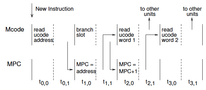
Figure 2 Microcode Timing Diagram
In t1,0 the address is loaded into MPC and in t1,1 it is sent back to
the Microcode unit to be used in t2,0 to read the first microcode word
for the new instruction in IR. There is thus a dead clock cycle in the
Microcode unit, identified as the branch slot in the figure. However,
unless the MPC receives an increment command, the Microcode unit will
read the same word again in the next clock cycle. Therefore, during
the branch slot, the Microcode unit automatically sends code to the
MPC unit to cause MPC to be incremented. As the Microcode unit reads
the first microcode word for the new instruction, MPC is incremented
to read the second.
If the instruction requires more than two microcode words, MPC must be
incremented once for each additional word and, for every instruction,
the last microinstruction to be executed must update PC. Except in the
case of a branch or jump instruction, PC must be incremented by +1. In
the case of a conditional branch, then depending on the outcome, a new
instruction can arrive in IR at the same time as a new
microinstruction. As noted earlier, this can happen during the
execution of branch instructions and if it does, a statement to this
effect appears in the Output Pane of the HASE window and the new
microinstriction is simply ignored.
It is important to remember that when an ALU operation is initiated,
the Condition Code bits should not be selected for use in a
conditional operation until the clock period after the ALU operation
has completed.
Using the Model
When first loaded, the model contains the microcode for the JUMP and
LD instructions, as shown in Table 4.
| Label | Microinstruction | Operand |
| JUMP | 20030000 | 0 |
| BRANCH | 00000000 | 0 |
| BEQZ | 00000000 | 0 |
| BNEG | 00000000 | 0 |
| JREG | 00000000 | 0 |
| LD | 10300000 | 38 |
| ... | | |
| ld | 20D00900 | 0 |
| 39 | 000000E0 | 0 |
| 40 | 000D4000 | 0 |
| ... | | |
Table 4. Initial Microcode
The Data Memory contains
values in each of its first 32 locations equal to their address. The
assembly code contained in the Instruction Memory consists of just two
instructions:
LD R2 5 // Loads R2 from data memory word 5
STOP // Stops the simulation
To add additional microcode and assembly code to the model, edit the
files called MICROCODE.Microcode.mem and
I_MEMORY.Instructions.mem. Then reload the model, re-run the
simulation and watch what happens.
When a simulation is run, the Output Pane of the HASE window records,
for each clock cycle, the current Microcode Memory address and the
codeword being processed. Sometimes this will be different from the
codeword at that address because it is overridden by zeros in a branch
slot.
Suggested Exercises
- Using only M-Format microinstructions, implement the
remaining microcode for instructions 0 - 25 and write an
appropriate assembly code program to demonstrate that they work.
- Using A-Format microinstructions, implement the multiply and
divide instructions and demonstrate that they work on suitable
test data, including all possible combinations of positive and
negative numbers. The microcode for divide the operations should
stop the simulation if an attempt is made to divide by zero.
- Implement OP1 and OP2 with functions of your own choice and
demonstrate that they work on suitable test data. An example
might be to form the sum of the first n natural numbers,
where n is the number in RS1 and the result is stored
in RD. Expect RS1 to be zero at the end of the operation.
Multiplication
The ALU is designed to be able to multiply together the numbers in A
and B by repeatedly adding the value in input B to the accumulator
(ACC). In each cycle, either the value in B or zero is added to ACC
according to the value of the least significant bit of A; A is then
shifted right one place and B is shifted left. The operation stops
when A becomes zero (whenever A is shifted, the Condition Code bits
are set according to the new value in A). This algorithm only works
for positive values of A. If A is initially negative, it must first be
negated and the final result negated before being returned to the
destination register.
Since the result of a multiply operation must not exceed 32 bits and
since the divide algorithm described below will only work with 16-bit
numbers, then whenever the ALU receives new operands for a multiply or
divide operation (as indicated by a boolean variable set in the
Microcode Unit), it checks its input values and stops the simulation
if one or other is out of range. Literal values are automatically
truncated to be in range, so these checks only matter for variables
read from the Data Memory.
Division
The ALU is designed to be able to divide 16-bit numbers by first
shifting the divisor in input B left 16 places and then repeatedly
subtracting it from the value in ACC, testing for a negative result
and shifting B right one place. If the result is negative, B is added
back to ACC before repeating the cycle. Unlike multiplication, where
the operation can be stopped when A becomes zero, division has to
continue for a full set of 17 cycles, counted down to zero by
decrementing and testing the value in register D. At the start of the
operation, the quotient in A is set to zero (this can be done by
loading from the bus but without sending a value to the bus
beforehand). After each subtraction, A is shifted left one place (as
described above, the value shifted into the least significant bit is
the inverse of CC1, (i.e. =1 if the value in ACC is
non-negative) and at the end of the operation contains the quotient of
the result, whilst the remainder is in ACC. However, there is no way
in EMMA to return each value to different register.
This algorithm only works for 16-bit positive numbers. The ALU checks
its input values and stops the simulation if they are out of range.
If either value is negative, it must be negated at the start and the
result negated, if appropriate, at the end. It’s also essential that
the microcode stops the simulation (by jumping to location 255) if an
attempt is to made to divide by zero.
Hints
- You will find it helps to use the Label field as exemplified in
the figure, i.e. in the jump table section the label identifies the
function whose numerical value corresponds to that address and in the
remainder of the microcode memory the label is either the address of
the location or the name of the instruction whose microcode starts at
that location. You can download microcode design sheets in
html or
pdf format.
- All fields in the microcode word (Label, Microcode, Operand) must
be filled.
- During development, some forms of error in the microcode can lead
to the simulation running for ever (as can forgetting the STOP
instruction at the end of the assembly code program). To prevent this
happening, the Microcode unit checks the current clock number against
the value of max_cycles and stops the simulation if it is exceeded.
max_cycles is set at the beginning of each simulation by the
statement max_cycles = 1 << log_max_cycles;
where log_max_cycles is a RANGE parameter set in the .edl file with a
range of 1-20 and an initial value of 11. To change this value, adjust
the slider as required before starting a simulation, then update the
.params file by clicking the parameters update icon
 in the top row of icons in the HASE window.
- When implementing MUL and DIV, it is helpful to draw flowcharts
before microcoding to show how the microcode will deal with
positive and negative values and in the case of DIV, a zero
denominator.
Return to Computer Architecture Simulation Models
HASE Project
Institute for Computing Systems Architecture, School of Informatics,
University of Edinburgh
Last change 13/2/2023