
This website describes the design of the 6600 processor and explains
how the HASE simulation model works. The most recent version of the
model (V3.1) includes a GLOBALS parameter Program that can be
edited after the model has been loaded into HASE. Program can
take values of 1, 2, 3 or 4 allowing the user to select one of two
programs contained in the model or one of two new programs added by
the user. After editing, clicking the "Write Parameters"
![]() updates the model's parameters file.
Program 1 in the model demonstrates the operation of many of the CDC
6600 instructions implemented in the model. Program 2 is a matrix
multiplication program - most early supercomputers were designed
specifically to perform well on this problem.
updates the model's parameters file.
Program 1 in the model demonstrates the operation of many of the CDC
6600 instructions implemented in the model. Program 2 is a matrix
multiplication program - most early supercomputers were designed
specifically to perform well on this problem.
The files for version 3 can be downloaded from cdc6600_v3.1.zip.
Instructions on how to use HASE models can be found at Downloading, Installing and Using HASE.
Figure 1 shows the organisation of the hardware of the 6600 central processor. In order to exploit the functional unit parallelism, the instruction set uses a three-address format (Figure 2) that allows successive instructions to refer to totally independent input and result operands. This would be quite impossible with a one-address instruction format, for example, where one of the inputs for an arithmetic operation is normally taken from, and the result returned to, a single implicit accumulator. Despite the potential for instruction overlap, dependencies between instructions can still occur in a three-address system. For example, where one instruction requires as its input the result of an immediately preceding instruction, the hardware must ensure that this ordering is strictly maintained. This would have been difficult if full store addresses were involved, since it would have made 6600 instructions prohibitively long, and it would in any case have been impossible to move operands in and out of Central Storage at a rate matching the execution rates of the functional units. The use of a small number of Scratch Pad Registers overcame both these problems.
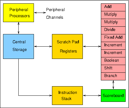
Figure 1. 6600 processor organisation
During program execution, instructions are taken in sequence from the Instruction Stack and issued by the Scoreboard to the appropriate execution unit. Each unit takes its input operands from among the 24 scratch-pad registers (eight 60-bit X (operand) registers, eight 18-bit A (address) registers, and eight 18-bit B (index) registers) and returns its result to one of these registers. The maximum rate of issue is one instruction per minor clock cycle (100 ns), while the units take typically 300 or 400 ns to complete their operations. Thus while the units can in principle all operate simultaneously, simultaneous operation of three or four units is more typical in practice. The issuing of instructions is not straightforward, since instruction dependencies can require that some instructions be held up until the completion of other, previously issued, instructions. In order to maximise the amount of concurrent processing, the Scoreboard is designed to issue each instruction as early as possible, within the limits set by these dependencies, so as to allow the following instruction to be issued, hopefully to a different unit. Dependency conflicts are resolved by the Scoreboard through control signals which link it to each unit and by the use of information buffered about the registers in respect of each unit and about the units in respect of each register.
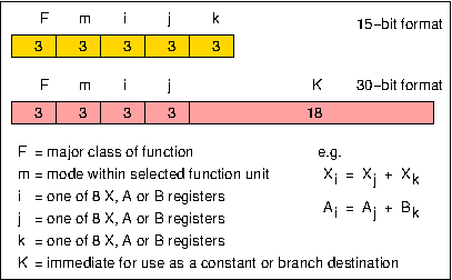
Figure 2. 6600 instruction format
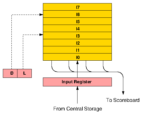
Figure 3. 6600 instruction stack
Instruction words are made up of four 15-bit parcels and as the first instruction word enters the bottom register of the stack (I0), the first two parcels within the word (starting from the left) are transferred into a series of instruction registers within the Scoreboard control logic. At the same time, a further instruction fetch is initiated. Two parcels are taken to allow for long format (30-bit) instructions. If the first parcel is a short format (15-bit) instruction, the second parcel is ignored and in the next processor minor cycle the second and third parcels are taken from I0. When a long instruction is encountered an extra minor cycle is spent skipping over the second half, so that dealing with one complete instruction word never takes less than four 100 ns minor cycles. This matches the rate at which instructions move into the stack. Whenever a new instruction fetch is initiated, the contents of the stack ripple upwards one register every half minor cycle, with the topmost location (I7) being overwritten first. At the end of four minor cycles the contents of I0 are moved up and I0 is then ready to receive a new instruction from the Input Register.
In practice the rate at which instructions could be accessed from Central Storage turned out to be lower than anticipated at the design stage, which meant that a new instruction word would not actually be available until after a total of eight minor cycles. Since the rate at which instructions are issued to the functional units cannot often be maintained at one per minor cycle, however, the overall effect of this delay on performance was not quite so bad as might be imagined, and when executing loops which can be contained within the stack, no Central Storage accesses for instructions are required at all.
When a conditional branch is decoded, a test for jump within stack is made. This involves subtracting the current program address from the branch address. If the absolute value of the result is less than seven words, and if the values in D and L indicate that the branch is to a location within the stack, no further store accesses are made for instruction words until instruction parcels are again taken from I0. Thus a branch may jump forwards or backwards within the stack and loops may be held in the stack in various forms.
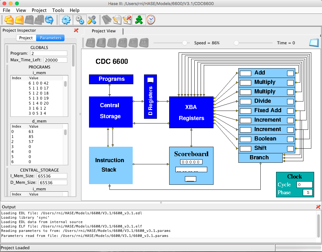
Figure 4. The CDC 6600 simulation model loaded into HASE
Also shown in Figure 5 are two entities that form part of the model rather than the 6600 itself, i.e. the standard HASE Clock entity and the Programs entity. Like the Central Storage entity, the Programs entity contains two arrays, one for instructions and one for (integer) data. Because memories in HASE are implemented as C++ arrays, the type-checking in C++ means that it is not possible to mix different types of element in a single array.
When downloaded, the Programs entity contains two programs, held in
the PROGRAMS.prog_mem.mem file at addresses starting at 0 and
256. After loading the project, the user can choose which program to
run by editing the GLOBALS parameter Program and updating the model's
parameter file by clicking the "Write Parameters" button
![]() . Users can add programs of their own, as programs 3/4,
in the PROGRAMS.prog_mem.mem file, starting at locations 512/768. The
data for each program is held in PROGRAMS.data_mem.mem file, each
program's data also starting at addresses 0/256/512/768.
. Users can add programs of their own, as programs 3/4,
in the PROGRAMS.prog_mem.mem file, starting at locations 512/768. The
data for each program is held in PROGRAMS.data_mem.mem file, each
program's data also starting at addresses 0/256/512/768.
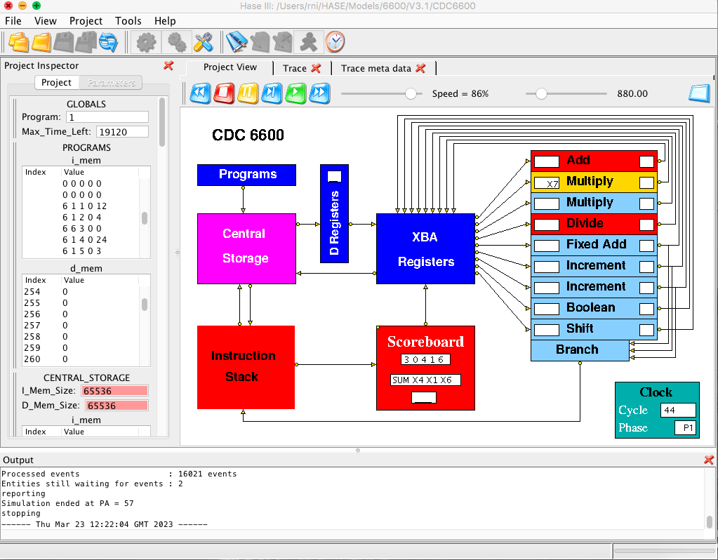
Figure 5. The CDC 6600 simulation model during animation
|
|
Table 1. 6600 instruction set
Operands are transferred between the X registers and Central Storage by instructions which load an address into registers A1-A5 (thus causing the corresponding operand to be read from that address in store and loaded into X1-X5), or into registers A6 or A7 (thus causing the contents of X6 or X7 to be transferred to that address in store). The 6600 had a complicated arrangement of data highways linking groups of the functional units and the registers, in order to balance performance against engineering and cost constraints. The HASE model simply provides whatever highways are needed.
The Instruction Stack in the model consists of eight registers (as in the real 6600) but each is only two instructions wide (for clarity in the display, instructions are held one per word in the memory of the model but are fetched in pairs from even/add addresses). This lack of verisimilitude is at least partly ameliorated by the fact that all instructions in the model are the same length, whereas, in the real 6600, programs contained a mixture of 15-bit and 30-bit instructions, so each register in the Instruction Stack might contain four instructions but would frequently only contain two or three. It also turns out that the inner loop of the matrix multiplication program in the model (progam 2) can be contained within the Instruction Stack, as would have been the case in the real 6600.
An important programming constraint imposed by the hardware design of the 6600 was that the target of a branch instruction could only be an instruction at the start of a 60-bit store word so, in the model, the target has to be an instruction at an even store address. In both systems, this can require the code to be padded out with PASS instructions, more about which can be found below.
The program is intended to demonstrate the operation of the architectural features of the central processor, in particular the way the scoreboard handles first, second and third order conflicts, as well as to test many of the instructions implemented in the model. Note that the instructions are not necessarily in the order that a simple compiler might have placed them but have been re-ordered to improve performance e.g. the instructions at PA = 15 and PA = 16. The first instruction tries (and fails) to load a non-zero value into B0 because B0 is defined in the architecture to always contain zero. Details about the remaining instructions are given in the descriptions of the functional units below the table.
| PA | F m i j k/K | Instruction | Action | Result |
| 0 | 6 1 0 0 42 | SUM of Bj and K to Bi | Tries to set B0 = 42 | B0 = 0 |
| 1 | 5 1 1 0 17 | SUM of Bj and K to Ai | A1 = B0 + 17 Loads X1 from CS 17 | A1 = 17 X1 = 513 |
| 2 | 5 1 2 0 18 | SUM of Bj and K to Ai | A2 = B0 + 18 Loads X2 from CS 18 | A2 = 18 X2 = 514 |
| 3 | 5 1 3 0 19 | SUM of Bj and K to Ai | A3 = B0 + 19 Loads X3 from CS 19 | A3 = 19 X3 = 515 |
| 4 | 5 1 4 0 20 | SUM of Bj and K to Ai | A4 = B0 + 20 Loads X4 from CS 20 | A4 = 20 X4 = 516 |
| 5 | 3 1 6 1 2 | FLOATING DIFFERENCE of Xj and Xk to Xi | X6 = X1 - X2 | X6 = -1 |
| 6 | 3 0 5 3 4 | FLOATING SUM of Xj and Xk to Xi | X5 = X3 + X4 | X5 = 1031 |
| 7 | 4 0 6 1 2 | FLOATING PRODUCT of Xj and Xk to Xi | X6 = X1 * X2 | X6 = 263682 |
| 8 | 3 0 6 4 5 | FLOATING SUM of Xj and Xk to Xi | X6 = X4 + X5 | X6 = 1547 |
| 9 | 4 4 7 6 4 | FLOATING DIVIDE Xj by Xk to Xi | X7 = X6 / X4 | X7 = 2 |
| 10 | 4 0 5 4 7 | FLOATING PRODUCT of Xj and Xk to Xi | X5 = X4 * X7 | X5 = 1032 |
| 11 | 3 0 4 1 6 | FLOATING SUM of Xj and Xk to Xi | X4 = X1 + X6 | X4 = 2060 |
| 12 | 5 1 1 0 0 | SUM of Bj and K to Ai | A1 = B0 + 0 Loads X1 from CS 0 | A1 = 0 X1 = 63 |
| 13 | 5 1 2 0 1 | SUM of Bj and K to Ai | A2 = B0 + 1 Loads X2 from CS 1 | A2 = 1 X2 = 85 |
| 14 | 1 1 6 1 2 | LOGICAL PRODUCT of Xj and Xk to Xi | X6 = X1 & X2 | X6 = 21 |
| 15 | 5 1 3 0 2 | SUM of Bj and K to Ai | A3 = B0 + 2 Loads X3 from CS 2 | A3 = 2 X3 = 57 |
| 16 | 5 1 6 0 3 | SUM of Bj and K to Ai | A6 = B0 + 3 Writes X6 to CS 3 | A6 = 3 CS 3 = 21 |
| 17 | 1 2 7 2 3 | LOGICAL SUM of Xj and Xk to Xi | X7 = X2 | X3 | X7 = 125 |
| 18 | 1 3 6 2 3 | LOGICAL DIFFERENCE of Xj and Xk to Xi | X6 = X2 ^ X3 | X6 = 108 |
| 19 | 5 1 7 0 4 | SUM of Bj and K to Ai | A7 = B0 + 4 Writes X7 to CS 4 | A7 = 4 CS 4 = 125 |
| 20 | 5 1 6 0 5 | SUM of Bj and K to Ai | A6 = B0 + 5 Writes X6 to CS 5 | A6 = 5 CS 5 = 108 |
| 21 | 1 4 7 1 2 | TRANSMIT Xk~ to Xi | X7 = X2k~ | X7 = -86 |
| 22 | 1 5 6 1 2 | LOGICAL PRODUCT of Xj and Xk~ to Xi | X6 = X1 & X2~ | X6 = 42 |
| 23 | 5 1 7 0 6 | SUM of Bj and K to Ai | A7 = B0 + 6 Writes X7 to CS 6 | A7 = 6 CS 6 = -86 |
| 24 | 5 1 6 0 7 | SUM of Bj and K to Ai | A6 = B0 + 7 Writes X6 to CS 7 | A6 = 7 CS 7 = 42 |
| 25 | 1 6 7 2 3 | LOGICAL SUM of Xj and Xk~ to Xi | X7 = X2 | X3 | X7 = -41 |
| 26 | 1 7 6 2 3 | LOGICAL DIFFERENCE of Xj and Xk~ to Xi | X6 = X2 ^ X3~ | X6 = -109 |
| 27 | 5 1 7 0 8 | SUM of Bj and K to Ai | A7 = B0 + 8 Writes X7 to CS 8 | A7 = 8 CS 8 = -41 |
| 28 | 5 1 6 0 9 | SUM of Bj and K to Ai | A6 = B0 +9 Writes X6 to CS 9 | CS 9 = -109 |
| 29 | 4 7 0 0 6 | SUM of 1's in Xk to Xi | X0 = no. of 1's in X6 | X0 = 28 |
| 30 | 1 0 7 1 0 | TRANSMIT Xj to Xi | Copies X1 to X7 | X7 = 63 |
| 31 | 4 0 6 4 5 | FLOATING PRODUCT OF Xj and Xk to Xi | X6 = X4 * X5 | X6 = 2125920 |
| 32 | 6 1 1 0 4 | SUM of Bj and K to Bi | B1 = B0 + 4 | B1 = 4 |
| 33 | 6 1 2 0 -3 | SUM of Bj and K to Bi | B2 = B0 + (-3) | B2 = -3 |
| 34 | 2 0 7 1 5 | SHIFT Xi LEFT jk places | Shifts X7 left 13 places | X7 = 33030144 |
| 35 | 2 0 6 2 3 | SHIFT Xi RIGHT jk places | Shifts X6 right 19 places | X6 = 259 |
| 36 | 2 2 4 1 0 | SHIFT Xi NOMINALLY LEFT Bj places | Shifts X4 left B1 places | X4 = 32960 |
| 37 | 2 2 5 2 0 | SHIFT Xi NOMINALLY LEFT Bj places | Shifts X5 right -B2 places | X5 = 129 |
| 38 | 2 3 4 2 0 | SHIFT Xi NOMINALLY RIGHT Bj places | Shifts X4 left -B2 places | X4 = 263680 |
| 39 | 2 3 5 1 0 | SHIFT Xi NOMINALLY RIGHT Bj places | Shifts X5 right B1 places | X5 = 8 |
| 40 | 5 1 7 0 10 | SUM of Bj and K to Ai | A7 = B0 + 10 Writes X7 to CS 10 | A7 = 10 CS 10 = 33030144 |
| 41 | 3 6 4 2 3 | INTEGER SUM of Xj and Xk to Xi | X4 = X2 + X3 | X4 = 142 |
| 42 | 5 1 6 0 11 | SUM of Bj and K to Ai | A6 = B0 + 11 Writes X6 to CS 11 | A6 = 11 CS 11 = 259 |
| 43 | 1 0 7 4 0 | TRANSMIT Xj to Xi | Copies X4 to X7 | X7 = 142 |
| 44 | 3 7 6 1 3 | INTEGER DIFFERENCE of Xj and Xk to Xi | X6 = X1 - X3 | X6 = 6 |
| 45 | 5 1 7 0 12 | SUM of Bj and K to Ai | A7 = B0 + 12 Writes X7 to CS 12 | A7 = 12 CS 12 = 142 |
| 46 | 5 1 6 0 13 | SUM of Bj and K to Ai | A6 = B0 + 13 Writes X6 to CS 13 | A6 = 13 CS 13 = 6 |
| 47 | 7 1 0 0 0 | SUM of Bj and K to Xi | X0 = B0 + 0 | X0 = 0 |
| 48 | 7 5 2 3 1 | DIFFERENCE of Aj and Bk to Xi | X2 = A3 - B4 | X2 = -2 |
| 49 | 0 3 0 0 52 | GO TO K IF Xj = zero | X0 = 0, so branch | PA = 52 |
| 50 | 0 3 1 1 56 | GO TO K IF Xj ≠ zero | X1 = 63, so branch | PA = 56 |
| 51 | 4 6 0 0 0 | PASS | ||
| 52 | 0 3 3 2 54 | GO TO K IF Xj = negative | X2 = -2, so branch | PA = 54 |
| 53 | 4 6 0 0 0 | PASS | ||
| 54 | 0 3 2 2 56 | GO TO K IF Xj = positive | X2 = -2, so don't branch | PA = 55 |
| 55 | 0 2 1 0 46 | GO TO K + Bi | branch to 46 + B1 | PA = 50 |
| 56 | 4 6 0 0 0 | PASS | ||
| 57 | 0 0 0 0 0 | STOP |
Table 2. The demonstration program
"In the design of this unit, one humorous incident stands out and should be related. The instruction codes shown above represent a very simple and convenient combination if code 46 is included. However, code 46 was selected as the PASS instruction. As the reader has perhaps already suspected, the PASS instruction design ended up triggering a complete Divide Sequence! Needless to say, this minor embarrassment was corrected."The significance of this, of course, is that PASS instructions occur quite often in compiled or hand-written machine code programs because of the requirement that branch target instructions be placed at the start of a 60-bit word.
Examples of these instructions (DIV, POP and PASS) are included in the Demonstration Program at instructions 9, 29 and 51/53/56 respectively.
The Fixed Add Unit is also used as a partner to the Branch Unit when the latter is executing a conditional branch instruction which depends on a value in an X register.
In the model, the Shift Unit just performs the simple shift left and shift right operations. Instruction 20 and 21 combine the j and k fields into a 2-octal-digit number that determines the shift distance, while instructions 22 and 23 use the value in Bj to determine the distance but also reverse the direction of the shift if the value in Bj is negative. Examples of these operations are included in the Demonstration Program as instructions 34 to 39.
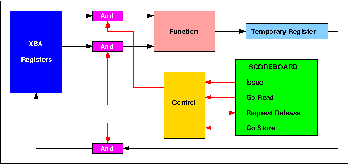
Figure 6. Control schematic for a 6600 functional unit
| X6 = X1 - X2 |
| X5 = X3 + X4 |
| X6 = X1 * X2 |
| X6 = X4 + X5 |
Both these conflicts are resolved by holding up the Issue signal for the second instruction until the first has completed. Issuing an instruction involves a sequence of four separate actions. Firstly, the functional unit required by the instruction is reserved by the setting of its busy flag, and the required operation, derived from the F and m fields of the instruction, is entered into it. No subsequent instruction can be sent to this unit until its busy flag has been re-set at the completion of the instruction which reserved it. Secondly, register designators Fi, Fj and Fk, derived from the i, j and k fields of the instruction, are copied into the functional unit in order to identify the operand and result registers which it will use. Thirdly, the Scoreboard copies into the current unit two numbers, Qj and Qk, taken from the identifier registers associated with these operand registers, and finally the identifier register associated with the result register is loaded with the unit number of the current unit. Thus a subsequent instruction which requires the content of this result register as an input operand will receive this unit number as a Q number, and a subsequent instruction which also requires this register as a result register will not be issued until the identifier has been cleared. The importance of Q numbers becomes clear when second order conflicts are considered.
In the model, the Scoreboard displays in its bottom panel the unit or register that is the cause of a first order conflict. The (octal) Q numbers used in the model correspond to those used in the real 6600, as shown in Table 3. The D Registers receive values from Central Storage destined for the corresponding X Registers.
| Q number | Functional Unit | Q number | Functional Unit |
| 00 | Branch | 08 | no result pending |
| 01 | Increment 1 | 09 | D Register 1 |
| 02 | Increment 2 | 10 | D Register 2 |
| 03 | Shift | 11 | D Register 3 |
| 04 | Boolean | 12 | D Register 4 |
| 05 | Divide | 13 | D Register 5 |
| 06 | Multiply 1 | 14 | Long Add |
| 07 | Multiply 2 | 15 | Add |
Table 3. Q Numbers
| X6 = X1 + X2 |
| X7 = X5 / X6 |
The sequence of events for the example above is as follows. The unit number of the Add Unit is entered into the identifier register of X6 when the first instruction is issued. When the second instruction is issued, this unit number is copied from the X6 identifier register into the Qk register in the Divide Unit. When the Add Unit completes its operation it sends its Request Release signal to the Scoreboard, and on receiving a Go Store response, sends a Release signal to all the other functional units. Because the Divide Unit has the unit number of the Floating Add Unit set in its Qk register, it detects this Release signal and sets the k operand Read Flag. Assuming that the Qj register contains the value 8 (indicating that there was no outstanding result destined for X5 at the time when the divide instruction was issued), the Read Flag for the j operand would have been set immediately, and the divide operation therefore starts as soon as the Read Flag for the k operand is set.
In the model, the left hand window shown as part of each unit displays the Fj or Fk designator of the register causing the second order conflict.
| X7 = X6 / X4 |
| X5 = X4 * X7 |
| X4 = X1 + X6 |
This interlock is achieved through use of the Read Flags. When the multiplication instruction is issued there are no reservations on X4, and its Read Flag is set immediately. This Read Flag remains set until the X7 Read Flag is set at the end of the division operation, after which the multiplication is started and both Read Flags are re-set. Thus the fact that the value in a particular register is required as an input operand by a previously issued, but as yet unstarted, instruction is indicated by the presence of a Read Flag for that register. Conversely, if there are no Read Flags set for a particular register, that register can be described as All Clear and a Go Store can be returned to a unit which is ready to send a result to it. The All Clear signal is produced by decoding the Fj and Fk operand designators for each unit and ANDing the decoder outputs with the corresponding Read Flag signal to produce an indication of whether or not the unit has a Read Flag set for a given register. For each register the signals from all the units are then combined to produce the All Clear signal indicating whether or not there are any Read Flags set for it. The Go Store signal for a particular unit is formed by decoding its Fi (result register) designator and combining together the results of AND operations between these decoded Fi signals and the corresponding All Clear signals for the registers.
In the example above the Fi designator for the Add Unit identifies register X4, and until the multiplication starts the Multiply Unit has a Read Flag set for X4, inhibiting the X4 All Clear signal. When the multiplication starts, this Read Flag is re-set, the X4 All Clear signal becomes true, and the Add Unit receives Go Store. It then sends its result and Fi value along a data highway to the XBA registers where the Fi value is decoded to control entry of the result into the appropriate register, and the clearing of the result reservation in the corresponding identifier register.
In the model, the right hand window shown as part of each unit displays the Fi designator of the register causing the third order conflict.
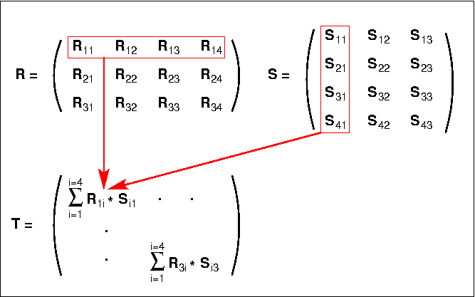
Figure 7. Matrix multiplication example
Table 4 shows the program contained in the model. It firsts sets up the required matrix parameters and variables in B registers, then fetches the elements of the first row of matrix R from memory and loads them into registers X1 - X4. It then fetches the elements of the first column of S in turn, loading each one into X5, forming the relevant sub-product in X6 using the values in X1 to X4 in turn, and adding each sub-product to the running total in X7. When all 4 sub-products have been added, the value in X7 is written to the first element of T. The T address is then incremented and the program loops back to start the second scalar product using elements of the second column of S.
Instructions 12 - 27 contain the unrolled loop calculating the scalar product of a row of matrix R and a column of matrix S. Instruction 27 tests whether all the columns of S have been processed for the current R row and branches back to instruction 12 if not. If they have, the next three instructions increment the R row number, move the current R element address to the start of the next row and reset the current S column number to zero. Instruction 31 tests whether all the rows of R have been processed and branches back to instruction 8 if not. The effective inner loop of this program is thus between instructions 12 and 27, i.e. 16 instructions in total. These instructions can be contained within the Instruction Stack, so for each R row, no instruction accesses to Central Storage occur during the second, third and fourth executions of this loop, as can be observed during animation of the model.
| PA | Instruction | Action | Comment | Result |
| 0 | 6 1 1 0 12 | B1 = B0 + 12 | B1 = address of first element of R | B1 = 12 |
| 1 | 6 1 2 0 4 | B2 = B0 + 4 | B2 = R row length | B2 = 4 |
| 2 | 6 6 3 0 0 | B3 = B0 + B0 | B3 = current R row | B3 = 0 |
| 3 | 6 1 4 0 24 | B4 = B0 + 24 | B4 = address of first element of S | B4 = 24 |
| 4 | 6 1 5 0 3 | B5 = B0 + 3 | B5 = S row length | B5 = 3 |
| 5 | 6 6 6 0 0 | B6 = B0 + B0 | B6 = current S column | B6 = 0 |
| 6 | 6 6 7 0 0 | B7 = B0 + B0 | B7 = element address in T | B7 = 0 |
| 7 | 4 6 0 0 0 | PASS | ||
| 8 | 5 6 1 1 0 | A1 = B1 + B0 | load X1 with first element of R row | X1 = 1, etc |
| 9 | 5 1 2 1 1 | A2 = B1 + 1 | load X2 with second element of R row | X2 = 2, etc |
| 10 | 5 1 3 1 2 | A3 = B1 + 2 | load X3 with third element of R row | X3 = 3, etc |
| 11 | 5 1 4 1 3 | A4 = B1 + 3 | load X4 with fourth element of R row | X4 = 4, etc |
| 12 | 5 6 5 4 6 | A5 = B4 + B6 | load X5 with first element of S column | X5 = 13, etc |
| 13 | 6 1 6 6 1 | B6 = B6 + 1 | increment B6 ready for next cycle | B6 = 1, etc |
| 14 | 4 0 6 1 5 | X6 = X1 * X5 | multiply X1 by X5 to form first sub-product | X5 = 12, etc |
| 15 | 5 4 5 5 5 | A5 = A5 + B5 | load X5 with second element of S column | X5 = 15, etc |
| 16 | 1 0 7 6 0 | X7 = X6 | load first sub-product into X7 | |
| 17 | 4 0 6 2 5 | X6 = X2 * X5 | multiply X2 by X5 to form second sub-product | |
| 18 | 5 4 5 5 5 | A5 = A5 + B5 | load X5 with third element of S column | |
| 19 | 3 0 7 7 6 | X7 = X7 + X6 | add second sub-product to sum | |
| 20 | 4 0 6 3 5 | X6 = X3 * X5 | multiply X3 by X5 to form third sub-product | |
| 21 | 5 4 5 5 5 | A5 = A5 + B5 | load X5 with fourth element of S column | |
| 22 | 3 0 7 7 6 | X7 = X7 + X6 | add third sub-product to sum | |
| 23 | 4 0 6 4 5 | X6 = X4 * X5 | multiply X4 by X5 to form fourth sub-product | |
| 24 | 3 0 7 7 6 | X7 = X7 + X6 | add fourth sub-product to sum | |
| 25 | 5 1 7 7 36 | A7 = B7 + 36 | write sum of products in X7 to element of T | |
| 26 | 6 1 7 7 1 | B7 = B7 + 1 | increment T address | |
| 27 | 0 5 6 5 11 | GO TO PA 12 if B6 ≠ B5 | start next scalar product if S column number < 3 | |
| 28 | 6 1 3 3 1 | B3 = B3 + 1 | increment R row number | |
| 29 | 6 6 1 1 2 | B1 = B1 + B2 | set R address to start of next row | |
| 30 | 6 6 6 0 0 | B6 = B0 + B0 | reset current S column number to 0 | |
| 31 | 0 5 3 5 7 | GO TO PA 8 if B3 ≠ B5 | read next row of R if row number < 3 | |
| 32 | 0 0 0 0 0 | STOP |
Table 4. The matrix multiplication program